Introduction
PCB design for manufacturability (DFM) is a vital part of the printed circuit board design process. This approach focuses on creating PCBs that are easy and cost-effective to manufacture, assemble, and test. This article delves into the best practices for DFM, aiming to streamline the PCB design process and enhance overall efficiency and reliability.
Understanding the Manufacturing Process
Gaining Insight into Production Capabilities
The foundation of successful PCB design for manufacturability lies in a thorough understanding of the manufacturing process and the capabilities of the manufacturing facility. This includes knowledge of the types of materials and technologies used, as well as the limitations and constraints of the manufacturing process. By understanding these factors, designers can make informed decisions to ensure that their PCB designs are optimized for manufacturability.
Utilizing Standard Components and Materials
Simplifying the Manufacturing Process
One key aspect of DFM is the use of standard components and materials. Standardization simplifies the manufacturing process and can significantly reduce costs. For instance, using standard resistors, capacitors, and materials like FR4 or FR5 minimizes the need for stocking and managing a large variety of unique components, thereby reducing manufacturing complexity and expense.
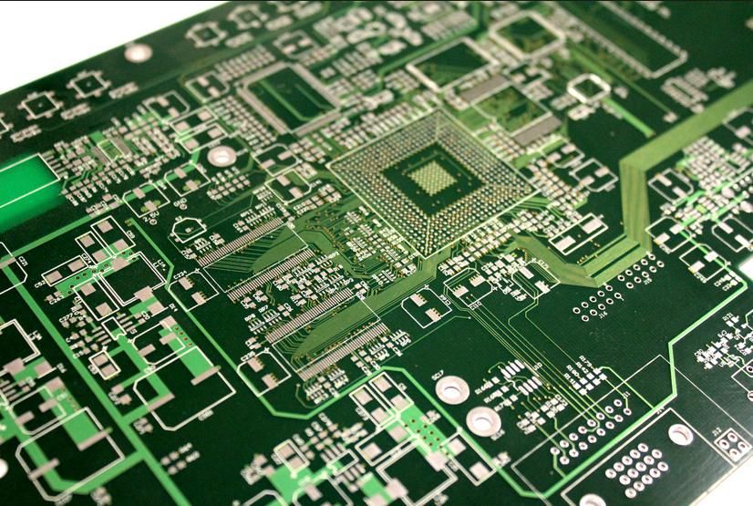
Optimizing PCB Layout
Designing for Ease of Manufacture and Assembly
A well-optimized PCB layout is crucial for manufacturability. This involves minimizing the number of vias and simplifying routing complexity, which can facilitate a more straightforward manufacturing process. Additionally, considering the thermal properties of components in the layout can mitigate thermal stress and potential damage during operation.
Incorporating Design for Test (DFT) Techniques
Facilitating Easier Testing and Debugging
Designing with testability in mind is another critical component of DFM. Incorporating DFT techniques, such as test points and test pads, makes it easier to access and test components on the PCB. This proactive approach can significantly reduce the time and costs associated with testing and debugging.
Implementing Design for Assembly (DFA) Techniques
Streamlining the Assembly Process
Design for assembly (DFA) focuses on simplifying the PCB assembly process. This involves using components with standard pinouts, incorporating surface mount technology (SMT) components, and reducing the number of components that require hand soldering. These practices can streamline assembly and population, cutting down on time and costs.
Emphasizing Design for Reliability (DFR)
Ensuring Long-Term Reliability and Durability
Reliability is a key consideration in DFM. Incorporating design for reliability (DFR) techniques involves selecting components with high reliability ratings, using effective thermal management strategies, and minimizing solder joints and potential failure points. This approach ensures that PCBs are robust and operate reliably over their intended lifespan.
Conclusion
PCB design for manufacturability is a critical aspect of the PCB design process. By comprehending the manufacturing process, utilizing standard components and materials, optimizing layout, incorporating DFT and DFA techniques, and emphasizing reliability, designers can create PCBs that are easy and cost-effective to produce, assemble, and test. Adhering to these best practices not only reduces design time and costs but also ensures that PCBs perform reliably and efficiently throughout their lifespan.
FAQs
Q: What is PCB Design for Manufacturability (DFM)?
A: PCB Design for Manufacturability (DFM) is a design approach focused on creating PCBs that are easy and cost-effective to manufacture, assemble, and test.
Q: Why is it important to use standard components and materials in PCB design?
A: Using standard components and materials simplifies the manufacturing process, reduces costs, and minimizes the complexity of stocking and managing various components.
Q: How does optimizing PCB layout contribute to DFM?
A: Optimizing PCB layout by minimizing vias, simplifying routing, and considering thermal properties helps streamline the manufacturing process and reduces the risk of damage during operation.
Q: What are Design for Test (DFT) techniques?
A: DFT techniques involve incorporating features like test points and test pads into the PCB design to facilitate easier access, testing, and debugging of components.
Q: What is the purpose of Design for Assembly (DFA) techniques?
A: DFA techniques aim to streamline the assembly process by using standard components, SMT technology, and reducing hand-soldered components, thereby saving time and reducing costs.
Q: How does Design for Reliability (DFR) impact PCB design?
A: DFR focuses on ensuring long-term reliability and durability of PCBs by using high-reliability components, effective thermal management, and minimizing potential failure points.