Bevezetés
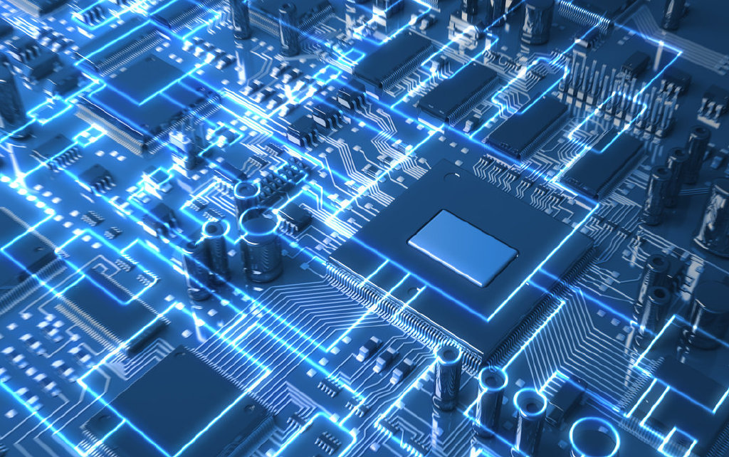
A nyomtatott áramköri lapok összeszerelési folyamata (PCBA) kulcsfontosságú lépés az elektronikus eszközök gyártásában. Ez a folyamat magában foglalja az elektronikus alkatrészek, például ellenállások, kondenzátorok és integrált áramkörök pontos elhelyezését a nyomtatott áramköri lapra (PCB), és annak biztosítását, hogy ezek összeköttetései funkcionális elektronikus áramkört alkossanak. Ez az aprólékos folyamat nagyfokú precizitást és odafigyelést igényel, mivel még a legkisebb hibák is hibás termékekhez vezethetnek.
A nyomtatott áramköri lap előkészítése
Tiszta és határozott felület biztosítása
Az összeszerelési folyamat kezdeti fázisa a nyomtatott áramköri lap előkészítése. A lapot alaposan megtisztítjuk, hogy eltávolítsunk minden olyan szennyeződést vagy törmeléket, amely zavarhatja az összeszerelési folyamatot. Ezután forrasztási maszkot visznek fel a lapra, hogy megvédjék azt a forraszanyag fröccsenésétől, és hogy körülhatárolják a pads és a süllyesztési pontokat. Ezt követően egy réteg forraszpasztát - amely forraszporból és folyósítószerből áll - viszünk fel, hogy biztosítsuk a forraszanyag egyenletes folyását.
Komponensek elhelyezése Pick-and-Place használatával
Pontosság az alkatrészek pozicionálásában
Miután a lapot előkészítették, a következő lépés az elektronikus alkatrészek elhelyezése a NYÁK-ra, ez a folyamat az úgynevezett pick-and-place. Ezt általában egy gép végzi, amely pontosan felveszi az alkatrészeket és elhelyezi őket a lapon. A gép biztosítja, hogy minden egyes alkatrész a megfelelő helyre kerüljön, figyelembe véve az alkatrészek méretét, alakját és tájolását.
A PCB-szerelvény tesztelése
Hibák felderítése és kijavítása
Miután minden alkatrész a helyére került, a lapot egy sor vizsgálatnak vetik alá, hogy ellenőrizzék annak épségét. Ezek a tesztek magukban foglalják a vizuális ellenőrzést, az elektromos teszteket és a funkcionális teszteket, amelyek célja az összeszerelési folyamat során keletkezett hibák vagy hibák, például a rosszul illesztett alkatrészek vagy hibás csatlakozások azonosítása.
Az alkatrészek forrasztása
Erős kötések létrehozása hullámforrasztással
A tesztelés után a lap a forrasztási fázisba kerül. A forraszpaszta megolvasztásához hőt alkalmaznak, amely erős kötést képez az alkatrészek és a lap között. Ezt a lépést általában hullámforrasztógéppel végzik, amely szabályozott mennyiségű hőt és nyomást alkalmaz.
Végső tesztelés és minőségbiztosítás
Teljes funkcionalitás biztosítása valós körülmények között
A forrasztást követően a lap további teszteknek vetik alá, hogy megerősítsék a teljes működőképességét. Ezek a tesztek további elektromos, funkcionális és környezeti teszteket tartalmaznak, például hőmérséklet- és páratartalom-ellenőrzést, hogy a kártya elviselje a normál használat során előforduló körülményeket.
A PCBA csomagolása és szállítása
A tábla védelme a szállításhoz
Miután a PCBA minden vizsgálaton megfelelt, becsomagolják és előkészítik a szállításra. Ez a lépés magában foglalja a kártya védőburkolatba vagy burkolatba helyezését és a szükséges kábelek vagy csatlakozók csatlakoztatását. A lap ezután készen áll a szállításra a megrendelőhöz, ahol egy teljes elektronikus eszközbe integrálják.
Következtetés
A PCBA összeszerelési folyamata összetett, rendkívül precíz eljárás, amely szakértelmet és aprólékos figyelmet igényel. A nyomtatott áramköri lap előkészítésétől a végső tesztelésig és csomagolásig minden egyes lépés döntő fontosságú annak biztosításához, hogy a lap teljesen működőképes és hibamentes legyen. Az összeszerelési folyamat megértésével a gyártók garantálhatják, hogy termékeik megfelelnek a legmagasabb minőségi és megbízhatósági követelményeknek.
GYIK
K: Mi az a PCBA?
V: A PCBA a nyomtatott áramköri lap összeszerelésének rövidítése, amely az elektronikus alkatrészek NYÁK-ra történő felhelyezésének és forrasztásának folyamatára utal, hogy egy működőképes elektronikus áramkört hozzanak létre.
K: Miért fontos a nyomtatott áramkör előkészítése?
V: A NYÁK előkészítése elengedhetetlen a tiszta felület biztosításához, a forraszanyag fröccsenése elleni védelemhez, valamint az alkatrészek elhelyezéséhez és a forrasztáshoz szükséges padok és síkok megfelelő meghatározásához.
K: Milyen szerepet játszik a pick-and-place gép a PCBA-ban?
V: A pick-and-place gép felelős az elektronikus alkatrészek pontos elhelyezéséért a NYÁK-on, figyelembe véve az egyes alkatrészek méretét, alakját és tájolását a pontos pozícionálás érdekében.
K: Hogyan azonosítják a hibákat a nyomtatott áramköri lapok összeszerelésénél?
V: A hibák azonosítása egy sor teszttel történik, beleértve a szemrevételezéses vizsgálatokat, elektromos teszteket és funkcionális teszteket, hogy felderítsék az olyan problémákat, mint a rosszul beállított alkatrészek vagy a hibás csatlakozások.
K: Mi az a hullámforrasztás?
V: A hullámforrasztás egy olyan eljárás, amely ellenőrzött hővel és nyomással olvasztja meg a forraszpasztát, erős kötéseket hozva létre az alkatrészek és a NYÁK között.
K: Miért fontos a végső tesztelés a PCBA-ban?
V: A végső tesztelés biztosítja, hogy a PCBA teljes mértékben működőképes legyen, és képes legyen ellenállni a valós körülményeknek, például a hőmérsékletnek és a páratartalomnak, biztosítva ezzel a lap megbízhatóságát.