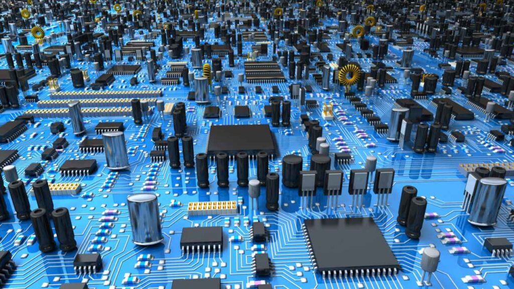
Printed Circuit Board (PCB) design is integral to modern electronics, forming the foundation of countless electronic devices by providing a precise and reliable platform to connect and support various components. This process requires a comprehensive understanding of fundamental principles, from material selection to software tools, to ensure the seamless functionality of complex electronics. This guide explores the core aspects of PCB design, including material selection, component placement, power distribution, signal integrity, manufacturing, and software utilization, offering insight into creating efficient and cost-effective PCBs.
Material Selection
The choice of materials is a crucial aspect of PCB design that directly impacts the performance and reliability of the final product. Key considerations include the substrate, copper thickness, and solder mask. A substrate with high thermal conductivity aids in dissipating heat generated by components, while inadequate copper thickness can compromise the board’s electrical integrity. Designers must carefully evaluate these factors to ensure the PCB meets specific performance requirements.
Component Placement and Routing
Strategic component placement and routing are vital for minimizing signal integrity issues, reducing electromagnetic interference (EMI), and optimizing thermal performance. This requires a thorough understanding of the electrical characteristics of components and the physical constraints of the PCB. Additionally, designers must consider mechanical integrity to ensure the board can withstand environmental stresses and handling.
Power Distribution Network (PDN) Design
A reliable and efficient power distribution network (PDN) is essential for delivering power to components. The PDN’s topology, component selection, and routing play a significant role in the board’s overall performance. Designers need to ensure the PDN meets the board’s power requirements while minimizing noise and voltage drops.
Signal Integrity (SI) System Design
The signal integrity (SI) system is responsible for transmitting and receiving signals between components, significantly impacting the board’s overall performance. The SI system’s topology, component selection, and routing must be carefully considered to meet signal integrity requirements and minimize noise and distortion.
Manufacturing and Assembly Considerations
Practical aspects of PCB design include manufacturing and assembly processes. Designers should consider these requirements to ensure efficient and cost-effective production. This involves selecting components that are easy to assemble, minimizing the number of solder joints, and optimizing the PCB layout for automated assembly.
Software Tools and Techniques
PCB design heavily relies on software tools and techniques, such as computer-aided design (CAD) software, simulation tools, and design for manufacturability (DFM) techniques. Proficiency in these tools is crucial for creating accurate designs, optimizing performance, and ensuring manufacturability. CAD software facilitates detailed designs, simulation tools analyze performance, and DFM techniques enhance layout and component placement.
Conclusion
PCB design is a complex and multifaceted process encompassing various technical and practical considerations. By mastering the fundamental principles of material selection, component placement and routing, power distribution, signal integrity, manufacturing, and software tools, designers can create PCBs that meet specifications, optimize performance, and minimize costs. This comprehensive approach ensures the creation of efficient, reliable, and cost-effective electronic devices.
FAQs
Q: Why is material selection important in PCB design?
A: Material selection, including substrate and copper thickness, directly affects the performance, thermal management, and electrical integrity of the PCB.
Q: How does component placement impact PCB design?
A: Effective component placement and routing minimize signal integrity issues, reduce EMI, optimize thermal performance, and ensure mechanical integrity.
Q: What is a Power Distribution Network (PDN) in PCB design?
A: The PDN delivers power to components. Its design, including topology and routing, is crucial for minimizing noise and voltage drops.
Q: Why is signal integrity important in PCB design?
A: Signal integrity ensures reliable signal transmission between components, impacting the board’s overall performance by minimizing noise and distortion.
Q: What role do software tools play in PCB design?
A: Software tools like CAD and simulation software help create accurate designs, optimize board performance, and ensure efficient manufacturability.