Introduction of PCBA Process In the manufacturing of electronic devices, the PCBA process is a crucial stage. During this process, components are attached to a printed circuit board (PCB) to create functional electronic products. Two key steps in the PCBA process are soldering and reflow, both of which require precision and control to ensure the final product’s […]
Author Archives: admin
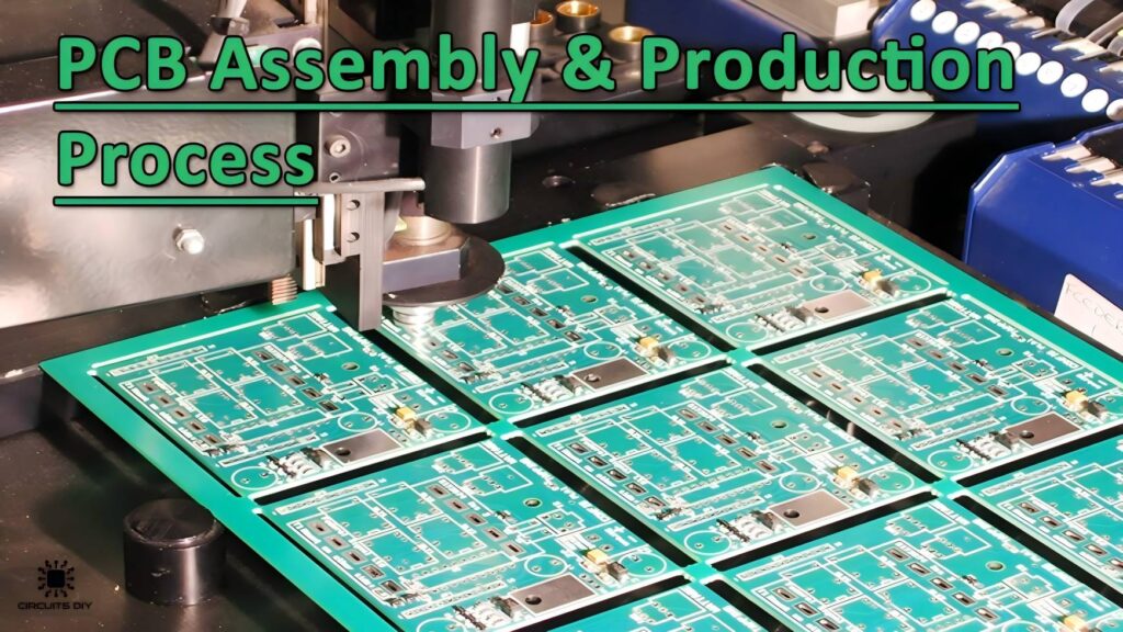
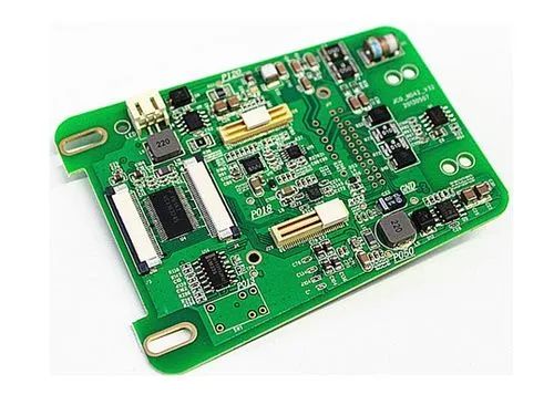
Introduction of PCBA Manufacturing PCBA manufacturing, or Printed Circuit Board Assembly manufacturing, is a vital process in the electronics industry. It involves assembling various electronic components onto a printed circuit board (PCB), transforming it into a fully functional electronic device. This complex process requires a high level of precision, expertise, and knowledge of electronic components […]
The Role of PCB Material in High-Frequency Applications Impact on System Performance The primary role of a PCB is to support and interconnect electronic components, but in high-frequency applications, the material of the PCB itself significantly influences system performance. High-frequency signals are highly sensitive to the PCB material’s properties, including dielectric constant, dissipation factor, and […]
Design Phase Creating the Digital Blueprint The PCB manufacturing process begins with the design phase, where engineers use specialized software to develop a detailed digital blueprint of the PCB. This design process must account for various factors, including the type of components, board layout, and electrical connections. After completing the initial design, it undergoes rigorous […]
Component Selection Choosing Components for Extreme Conditions One of the most critical aspects of designing for reliability is selecting the right components. For high-reliability applications, components must endure extreme temperatures, humidity, vibration, and resist corrosion and contamination. Designers must carefully choose components that meet these rigorous requirements and are qualified for high-reliability environments to ensure […]
Increasing Power Density Addressing Heat Generation in Compact Devices One of the foremost challenges in PCB thermal management is the rising power density of modern electronic devices. As components like CPUs, GPUs, and memory chips become more powerful and compact, the heat they generate can exceed the capacity of traditional cooling mechanisms. This can lead […]
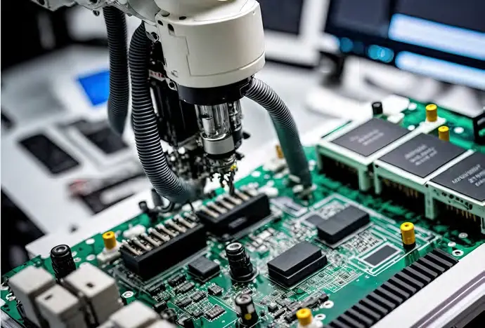
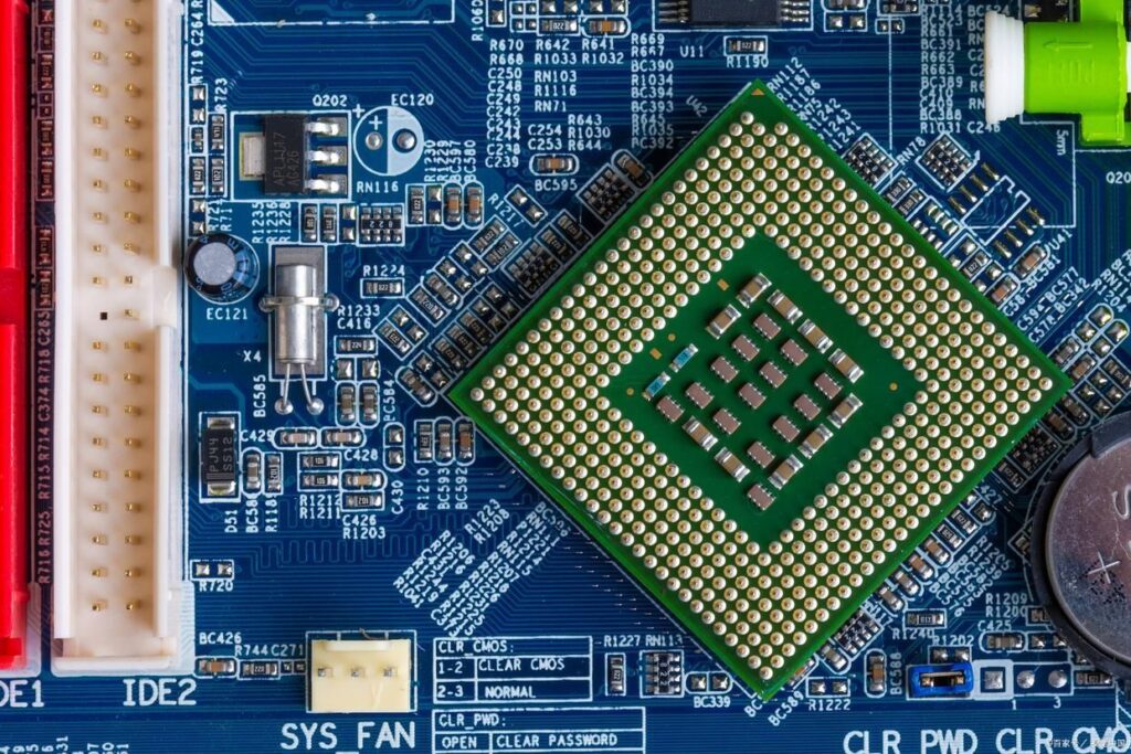
Increased Component Density Maximizing Space Efficiency One of the primary benefits of SMT is its ability to increase the density of components on a PCB. SMT allows manufacturers to place more components onto a smaller area, resulting in more compact and efficient devices. This capability has been instrumental in developing sophisticated electronics such as smartphones […]
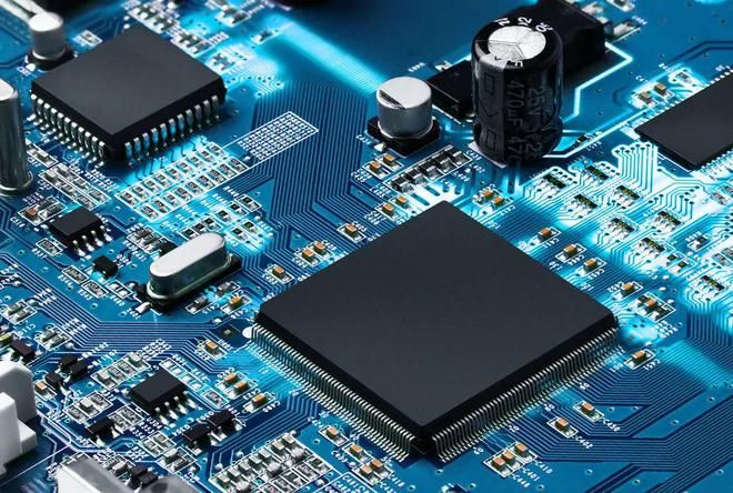
Understanding the Physical Properties and Electromagnetic Interactions Signal Integrity Challenges Designing high-speed digital circuits requires a thorough understanding of PCB materials and electromagnetic interactions. Signal integrity is a major concern; signal reflections can lead to errors and reduced performance. To mitigate this, designers use advanced techniques such as differential signaling and termination resistors. Differential signaling […]
The Soldering Process Preparation of Components and PCB The soldering process begins with thorough preparation. The PCB is cleaned to remove any impurities and oxidation, and flux is applied to aid in soldering. Components are inspected and cleaned to ensure they are free of defects. Solder paste, which combines solder powder and flux, is then […]
The Role of Electrical Testing and Inspection Ensuring Integrity and Functionality Electrical testing and inspection are vital processes in the quality assurance of PCBA. This process begins with a visual inspection to identify visible defects, such as cracks, scratches, or misaligned components. Following this, a series of electrical tests are conducted, including continuity, insulation, and […]