Technical Parameters about PCB and PCBA
| Item | Capability |
|---|---|
| Quality Standard | Standard IPC 2 |
| Layers | 1-32 Layers |
| Raw Material | ▪FR4 ▪CEM3 ▪Rogers ▪Teflon ▪Metal-based |
| Max Size | ▪850mm*520mm |
| Min Drill Diameter | 0.15mm |
| Copper thickness | 0.25OZ-15OZ |
| Impedance Tolerance | ±5% |
| Surface Finish | ▪Lead-free HASL ▪OSP ▪ENIG ▪Gold Plating ▪Immersion Ag/Sn |
| Item | Capability |
|---|---|
| Quality Standard | IPC-610-C |
| Assembly Technology | ▪SMT Stencil ▪SMT ▪DIP ▪Conformal Coating |
| Enterprise Certification | ▪ISO9001 ▪IATF16949 ▪ISO13485 ISO14001 |
| Product Certification | ▪UL ▪RoHS ▪SGS ▪REACH |
| SMD Capability | ▪Minimum size:01005 ▪BGA0.2mm, QFN, CSP, CON ▪ Maximum PCB:510*460mm |
| Value-added features | ▪Component procurement ▪NPI Report ▪PCBA Prototype ▪IC Programming ▪Repair |
| Testing process | ▪AOI ▪X-ray ▪SPI ▪FAI ▪FCT ▪ICT ▪Aging test ▪QC Manual detection |
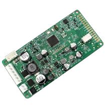
Application areas of PCBA
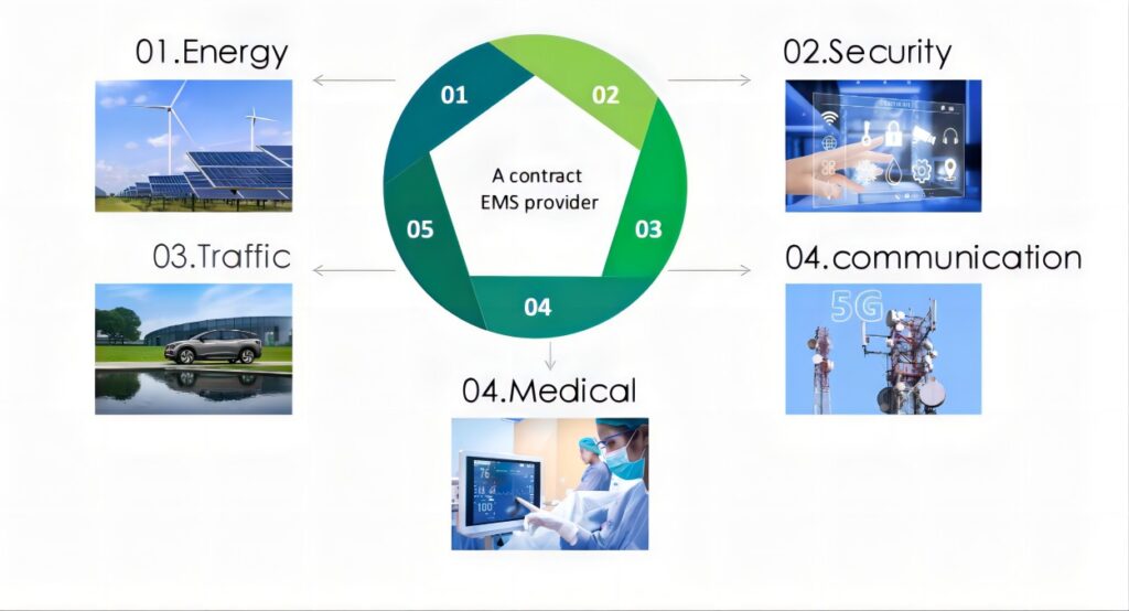
Specific applications of PCBA
Security System
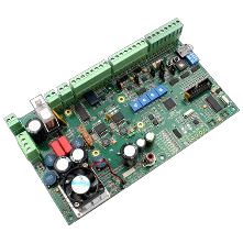

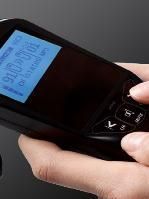
Communication Device
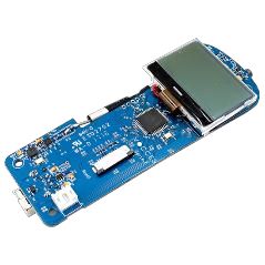
Driverless System
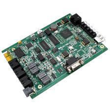

New Energy System
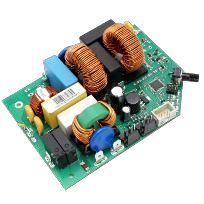

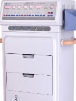
Medical Device
FAQ of PCB and PCBA Applications
1. What industries use PCBA applications?
PCBA applications include consumer electronics, automotive, aerospace, medical devices, telecommunications, and industrial automation.
2. What are the key components used in PCBA?
Key components include resistors, capacitors, diodes, transistors, integrated circuits (ICs), connectors, and inductors.
3. What testing methods are used in PCBA?
Common testing methods include In-Circuit Testing (ICT), Functional Testing (FCT), Automated Optical Inspection (AOI), and X-ray inspection.
4. What are the challenges in PCBA manufacturing?
Challenges include ensuring solder joint reliability, managing high component density, minimizing electromagnetic interference (EMI), and achieving precise component placement.