Introduction
The manufacturing of printed circuit boards (PCBs) is a meticulous process that necessitates precision and a comprehensive understanding of the numerous stages involved. Each step, from the initial design to the final assembly, is crucial in crafting a high-quality PCB. This guide provides a detailed overview of the PCB manufacturing process, highlighting the various techniques, materials, and technologies used in producing these essential electronic components.
Design Phase
Blueprint Creation and Prototyping
The PCB manufacturing journey begins with the design phase, where engineers and designers create a detailed blueprint. This blueprint considers various factors, including component placement, wiring, and layer thickness. After the blueprint is completed, a physical prototype is developed and tested to ensure it meets the necessary specifications. The finalized design then paves the way for the manufacturing process.
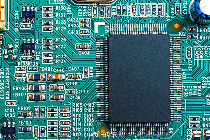
Substrate Creation and Etching
Creating the Foundation
The first step in manufacturing is creating the PCB substrate, usually made from materials like FR4 or FR5. A thin layer of copper is applied to this substrate, serving as the conductive material for the PCB. The copper layer undergoes a chemical etching process, forming the desired pattern of conductive paths and pads.
Drilling and Milling
Preparing for Components and Wiring
The PCB then undergoes a series of drilling and milling operations to create the required holes and cavities for components and wiring. This precise operation ensures that the PCB can accommodate the components and maintain proper electrical connectivity.
Solder Mask Application
Protecting and Preparing the PCB
A solder mask is applied next, protecting the copper layers from oxidation and ensuring smooth solder flow during assembly. The solder mask is essential for maintaining the integrity of the PCB’s conductive pathways.
Silkscreen Layer Application
Guiding the Assembly Process
The silkscreen layer provides a visual guide for the PCB’s layout and component placement. Made from a thin film of ink or paint, this layer assists in the accurate and efficient assembly of the PCB.
Component Assembly and Soldering
Bringing the PCB to Life
With the substrate and layers in place, the assembly process begins. Components are placed onto the PCB using a combination of manual and automated techniques. The components are then soldered in place using methods such as wave soldering and reflow soldering.
Testing and Inspection
Ensuring Quality and Reliability
Once assembled, the PCB undergoes rigorous testing and inspection to ensure it meets the required specifications. This phase may include visual inspections, electrical testing, and environmental testing to simulate real-world conditions.
Packaging and Shipping
Delivering the Finished Product
The final stage of the PCB manufacturing process involves packaging and shipping the finished PCBs. This includes wrapping the PCB in protective materials like foam or bubble wrap and placing it in a sturdy container for safe transport.
Conclusion
The PCB manufacturing process is a complex procedure that demands precision, attention to detail, and a thorough understanding of each stage. By mastering the various techniques, materials, and technologies involved, engineers and designers can produce PCBs that meet specifications and perform reliably in diverse applications.
FAQs
Q: What is the importance of the design phase in PCB manufacturing?
A: The design phase is crucial as it establishes the blueprint for the PCB, considering factors like component placement and wiring, which are essential for creating a functional and reliable PCB.
Q: Why is etching a critical step in PCB manufacturing?
A: Etching is vital because it creates the conductive pathways and pads on the PCB, allowing for proper electrical connectivity between components.
Q: How does the solder mask contribute to the PCB’s functionality?
A: The solder mask protects the copper layers from oxidation and ensures smooth solder flow during assembly, maintaining the integrity of the PCB’s conductive pathways.
Q: What are the primary methods of soldering in PCB assembly?
A: The primary methods of soldering in PCB assembly include wave soldering and reflow soldering, both of which secure components to the PCB effectively.
Q: What types of testing are performed on PCBs during manufacturing?
A: PCBs undergo various testing, including visual inspections, electrical testing, and environmental testing, to ensure they meet specifications and can perform reliably under different conditions.